
Products Category
- FM Transmitter
- 0-50w 50w-1000w 2kw-10kw 10kw+
- TV Transmitter
- 0-50w 50-1kw 2kw-10kw
- FM Antenna
- TV Antenna
- Antenna Accessory
- Cable Connector Power Splitter Dummy Load
- RF Transistor
- Power Supply
- Audio Equipments
- DTV Front End Equipment
- Link System
- STL system Microwave Link system
- FM Radio
- Power Meter
- Other Products
- Special for Coronavirus
Products Tags
Fmuser Sites
- es.fmuser.net
- it.fmuser.net
- fr.fmuser.net
- de.fmuser.net
- af.fmuser.net ->Afrikaans
- sq.fmuser.net ->Albanian
- ar.fmuser.net ->Arabic
- hy.fmuser.net ->Armenian
- az.fmuser.net ->Azerbaijani
- eu.fmuser.net ->Basque
- be.fmuser.net ->Belarusian
- bg.fmuser.net ->Bulgarian
- ca.fmuser.net ->Catalan
- zh-CN.fmuser.net ->Chinese (Simplified)
- zh-TW.fmuser.net ->Chinese (Traditional)
- hr.fmuser.net ->Croatian
- cs.fmuser.net ->Czech
- da.fmuser.net ->Danish
- nl.fmuser.net ->Dutch
- et.fmuser.net ->Estonian
- tl.fmuser.net ->Filipino
- fi.fmuser.net ->Finnish
- fr.fmuser.net ->French
- gl.fmuser.net ->Galician
- ka.fmuser.net ->Georgian
- de.fmuser.net ->German
- el.fmuser.net ->Greek
- ht.fmuser.net ->Haitian Creole
- iw.fmuser.net ->Hebrew
- hi.fmuser.net ->Hindi
- hu.fmuser.net ->Hungarian
- is.fmuser.net ->Icelandic
- id.fmuser.net ->Indonesian
- ga.fmuser.net ->Irish
- it.fmuser.net ->Italian
- ja.fmuser.net ->Japanese
- ko.fmuser.net ->Korean
- lv.fmuser.net ->Latvian
- lt.fmuser.net ->Lithuanian
- mk.fmuser.net ->Macedonian
- ms.fmuser.net ->Malay
- mt.fmuser.net ->Maltese
- no.fmuser.net ->Norwegian
- fa.fmuser.net ->Persian
- pl.fmuser.net ->Polish
- pt.fmuser.net ->Portuguese
- ro.fmuser.net ->Romanian
- ru.fmuser.net ->Russian
- sr.fmuser.net ->Serbian
- sk.fmuser.net ->Slovak
- sl.fmuser.net ->Slovenian
- es.fmuser.net ->Spanish
- sw.fmuser.net ->Swahili
- sv.fmuser.net ->Swedish
- th.fmuser.net ->Thai
- tr.fmuser.net ->Turkish
- uk.fmuser.net ->Ukrainian
- ur.fmuser.net ->Urdu
- vi.fmuser.net ->Vietnamese
- cy.fmuser.net ->Welsh
- yi.fmuser.net ->Yiddish
What is P-Channel MOSFET : Working and Its Characteristics
Date:2021/10/18 21:55:58 Hits:
P-Channel MOSFET is a classification of Metal Oxide Semiconductor Device. This consists of the n-substrate in the middle with light doping concentration. These are the three terminals devices. It possesses uni-polar characteristics because its operation is dependent on the majority of the charge carriers. In this, the majority of the carriers are holes because of two p materials utilized in the circuitry. It is further classified based on the existence of the channels. If the channel exists by default then it is known as depletion mode of the p-channel or if the channel is induced due to the voltage applied then it is known as enhancement mode of the p-channel.What is P-Channel MOSFET?A MOSFET formed when a lightly doped N-type substrate is connected to the two P-type materials which are highly doped. Doping means the amount concentration of the impurities added to the atom. 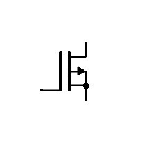 The p-channel formed in between the two P-type substrate can be either due to the induced voltages or it might already exists in prior.Based on this the p-channel MOSFET’s are classified as (1) P-channel with the Enhancement MOSFET(2) P-channel with the Depletion MOSFET WorkingThe working of the P-channel MOSFET is based on the channel formed/exists and the concentration of the majority charge carriers in the channel. In this case, the majority carriers are the holes.P Channel with Enhancement MOSFETThis MOSFET is designed with the n-substrate which is lightly doped. The two heavily doped p type materials are separated by the length (L). This L is known as the channel length. The thin layer of type silicon dioxide is deposited above the substrate. This layer is generally known as the dielectric layer. The two P type forms the source and the drain respectively. The aluminum which is used as the plating above the dielectric forms the gate terminal. The source and the MOSFET’s body is connected to the ground.A negative voltage has been applied to the gate terminal. Due to the effect of the capacitance, the positive concentration of the charges gets settle below at the layer called dielectric. The electrons that present at the n substrate due to the repulsive forces get shifted and the uncovered value of the positive ions layer can be found there. The holes which are minority carriers in n-type susbstrate combines with few of the electrons to form a bond.But on further application of the negative voltage breaks the covalent bonds and thereby the pairs formed between electron and holes breaks. This formation leads to the generation of the holes and leads to the increment in the carrier concentration of holes in the channel. When a negative voltage is applied to the drain terminal the channel becomes conductive hence the flow of the current occurs in the transistor.P Channel Depletion MOSFETThe formation of p channel depletion is just in reverse as compared with the n channel depletion MOSFET. Here the channel is pre-build due to the impurities of the p-type present in it. When the negative value of the voltage is applied at the terminal gate the free holes that represent the minority carriers at the n-type gets attracted towards the channel of the impurity ions of positive type. Under this condition when a drain terminal is reverse biased the device starts conducting but as the negative voltage in the drain terminal is increased it results in the formation of the depletion layer.This region is dependent on the concentration of the layer formed due to the positive ions. The width of the region of depletion affects the value of the conductivity of the channel. By variations of the voltage value of the region, the current at the terminal gets controlled. Finally, the gate and the drain remain at the negative polarity whereas the source remains at the zero value. Please refer to this link to know more about MOSFET MCQsP Channel MOSFET CharacteristicsThe MOSFET’s represents the voltage controlled devices.The input impedance values of these devices are high.In P-channel the conductivity of the channel is due to the negative polarity application at the gate terminal.The value of Drain current tends to increase but in terms of the reverse direction but the value of the voltage at drain and source seems to decrease. This represents the device operating in the ohmic region.The characteristics of the p channel are similar to that of the n channel but only the difference of the polarities is the matter because the substrates values are different here.Now can you tell which one is most preferable during the applications of amplification either n- channel or p-channel?
Leave a message
Message List
Comments Loading...
