
Products Category
- FM Transmitter
- 0-50w 50w-1000w 2kw-10kw 10kw+
- TV Transmitter
- 0-50w 50-1kw 2kw-10kw
- FM Antenna
- TV Antenna
- Antenna Accessory
- Cable Connector Power Splitter Dummy Load
- RF Transistor
- Power Supply
- Audio Equipments
- DTV Front End Equipment
- Link System
- STL system Microwave Link system
- FM Radio
- Power Meter
- Other Products
- Special for Coronavirus
Products Tags
Fmuser Sites
- es.fmuser.net
- it.fmuser.net
- fr.fmuser.net
- de.fmuser.net
- af.fmuser.net ->Afrikaans
- sq.fmuser.net ->Albanian
- ar.fmuser.net ->Arabic
- hy.fmuser.net ->Armenian
- az.fmuser.net ->Azerbaijani
- eu.fmuser.net ->Basque
- be.fmuser.net ->Belarusian
- bg.fmuser.net ->Bulgarian
- ca.fmuser.net ->Catalan
- zh-CN.fmuser.net ->Chinese (Simplified)
- zh-TW.fmuser.net ->Chinese (Traditional)
- hr.fmuser.net ->Croatian
- cs.fmuser.net ->Czech
- da.fmuser.net ->Danish
- nl.fmuser.net ->Dutch
- et.fmuser.net ->Estonian
- tl.fmuser.net ->Filipino
- fi.fmuser.net ->Finnish
- fr.fmuser.net ->French
- gl.fmuser.net ->Galician
- ka.fmuser.net ->Georgian
- de.fmuser.net ->German
- el.fmuser.net ->Greek
- ht.fmuser.net ->Haitian Creole
- iw.fmuser.net ->Hebrew
- hi.fmuser.net ->Hindi
- hu.fmuser.net ->Hungarian
- is.fmuser.net ->Icelandic
- id.fmuser.net ->Indonesian
- ga.fmuser.net ->Irish
- it.fmuser.net ->Italian
- ja.fmuser.net ->Japanese
- ko.fmuser.net ->Korean
- lv.fmuser.net ->Latvian
- lt.fmuser.net ->Lithuanian
- mk.fmuser.net ->Macedonian
- ms.fmuser.net ->Malay
- mt.fmuser.net ->Maltese
- no.fmuser.net ->Norwegian
- fa.fmuser.net ->Persian
- pl.fmuser.net ->Polish
- pt.fmuser.net ->Portuguese
- ro.fmuser.net ->Romanian
- ru.fmuser.net ->Russian
- sr.fmuser.net ->Serbian
- sk.fmuser.net ->Slovak
- sl.fmuser.net ->Slovenian
- es.fmuser.net ->Spanish
- sw.fmuser.net ->Swahili
- sv.fmuser.net ->Swedish
- th.fmuser.net ->Thai
- tr.fmuser.net ->Turkish
- uk.fmuser.net ->Ukrainian
- ur.fmuser.net ->Urdu
- vi.fmuser.net ->Vietnamese
- cy.fmuser.net ->Welsh
- yi.fmuser.net ->Yiddish
What is Enhancement MOSFET & Its Operation
Date:2021/10/18 21:55:57 Hits:
Transistors are the most popular semiconductors in the field of electronics. These are available in various types and configurations such as Bipolar-Junction Transistors (BJTs) and the Field-Effect Transistors (FETs) considered as the basic ones. These FETs are further classified as Junction field-effect transistors (JFET) and insulated gate field-effect transistors (IGFET). The transistor with input at the gate is insulated electrically from the main channel of current-carrying is referred to as IGFET or the metal oxide field-effect transistor (MOSFET). The electrode at the gate of these MOSFETs is made up of metal oxide. These MOSFETs operate in two modes and are classified as Enhancement MOSFET and Depletion MOSFET.What is Enhancement MOSFET?MOSFETs are usually classified into two types. They are Enhancement and the Depletion MOSFETs. The MOSFET that is basically in OFF condition which requires a certain amount of voltage at the terminal gate to turn ON is referred to as Enhancement MOSFET. Due to the application of gate voltage the channel among the terminal of drain and source gets less resistive. If the applied voltage at the gate increases then the current flow from the terminals drain to the source increases until and unless it reaches its maximum point. The behavior of this type of MOSFET resembles the behavior of bipolar junction transistor (BJT).The Schematic symbol of Enhancement MOSFETs of both p-channel and n-channel MOSFETs are: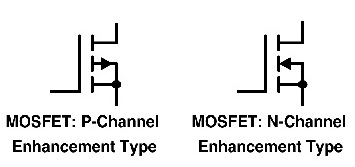 Enhancement MOSFET Symbol ConstructionThe steps involved in the construction of Enhancement MOSFET are:Two N regions separated by a distance of 25 micrometers with heavy doping concentration are diffused on a lightly doped substrate of p-type. Those N-regions are enacted as the terminals drain and source.Over the surface, a thin layer of insulation called silicon dioxide is developed. The holes made on this layer establishes aluminum contacts for the terminal’s source and the drain.This layer of conduction acts as the terminal gate. It is laid over the silicon dioxide and on the entire area of the channel.But it doesn’t have any physical channel for conduction.The p-type substrate extended over the entire silicon dioxide layer in this type of enhancement MOSFET.
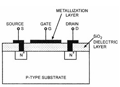 Enhancement MOSFET DiagramOperation of an Enhancement MOSFETThe operation of the Enhancement MOSFET areTo induce the channel positive polarity of the Gate to Source voltage is required. A large amount of voltage must be applied at the terminal gate for this operation.If the voltage applied at the terminals gate to the source is zero, Enhancement MOSFET doesn’t conduct. This can be the reason it is initially in the OFF condition.When the applied amount voltage at the terminal gate exceeds the limit of the threshold the current at the drain tends to flow through the circuit.Let us consider a situation when the positive amount of the voltage applied at the Drain- Source by keeping the gate voltage as zero. In this situation, the p-type of the substrate and the two N-regions behave like the two junctions of PN.This makes both the junctions reverse bias and the leakage current tends to flow through the circuit.Now if the voltage applied at the gate is made positive. The minority carriers present in the substrate of p-type (that is electrons) get attracted to the positive potential of the terminal gate.These negative charge carriers get accommodated below the terminal of the gate. Further increment in the VGS will deposit more amount of carriers called electrons.The use of dielectric prevents the movement of these electrons across the layer of silicon dioxide.This accumulation results in the formation of the n-channel amid Drain-Source.This leads to the generated drain current flow through the channel. This drain current is proportional to the resistance of the channel which is further dependent upon the carriers attracted towards the positive terminal of the gate.Hence from the above points, it can be concluded that the channel conduction is enhanced based on the positive potential of the gate terminal.Please refer to this link to know more about MOSFET MCQsDrain Characteristics of Enhancement MOSFETThe amount of current flow is dependent on the positive amount of the potential applied at the terminal gate. If the application of the potential is below the threshold then no current flow is evident through the terminal drain. If the voltage exceeds the threshold the device gets turned ON.
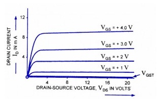 Drain CharacteristicsThe Enhancement type MOSFET is well suited in the application areas where power devices are used. To increase the conductivity the amount of applied gate potential must also be increased. Because of the low resistance required to turn ON the device and high resistance offered while turning it OFF these devices are preferred for switching applications. After knowing the applications of Enhancement MOSFETs can you describe where the depletion-mode MOSFET is preferred?
Leave a message
Message List
Comments Loading...
