
Products Category
- FM Transmitter
- 0-50w 50w-1000w 2kw-10kw 10kw+
- TV Transmitter
- 0-50w 50-1kw 2kw-10kw
- FM Antenna
- TV Antenna
- Antenna Accessory
- Cable Connector Power Splitter Dummy Load
- RF Transistor
- Power Supply
- Audio Equipments
- DTV Front End Equipment
- Link System
- STL system Microwave Link system
- FM Radio
- Power Meter
- Other Products
- Special for Coronavirus
Products Tags
Fmuser Sites
- es.fmuser.net
- it.fmuser.net
- fr.fmuser.net
- de.fmuser.net
- af.fmuser.net ->Afrikaans
- sq.fmuser.net ->Albanian
- ar.fmuser.net ->Arabic
- hy.fmuser.net ->Armenian
- az.fmuser.net ->Azerbaijani
- eu.fmuser.net ->Basque
- be.fmuser.net ->Belarusian
- bg.fmuser.net ->Bulgarian
- ca.fmuser.net ->Catalan
- zh-CN.fmuser.net ->Chinese (Simplified)
- zh-TW.fmuser.net ->Chinese (Traditional)
- hr.fmuser.net ->Croatian
- cs.fmuser.net ->Czech
- da.fmuser.net ->Danish
- nl.fmuser.net ->Dutch
- et.fmuser.net ->Estonian
- tl.fmuser.net ->Filipino
- fi.fmuser.net ->Finnish
- fr.fmuser.net ->French
- gl.fmuser.net ->Galician
- ka.fmuser.net ->Georgian
- de.fmuser.net ->German
- el.fmuser.net ->Greek
- ht.fmuser.net ->Haitian Creole
- iw.fmuser.net ->Hebrew
- hi.fmuser.net ->Hindi
- hu.fmuser.net ->Hungarian
- is.fmuser.net ->Icelandic
- id.fmuser.net ->Indonesian
- ga.fmuser.net ->Irish
- it.fmuser.net ->Italian
- ja.fmuser.net ->Japanese
- ko.fmuser.net ->Korean
- lv.fmuser.net ->Latvian
- lt.fmuser.net ->Lithuanian
- mk.fmuser.net ->Macedonian
- ms.fmuser.net ->Malay
- mt.fmuser.net ->Maltese
- no.fmuser.net ->Norwegian
- fa.fmuser.net ->Persian
- pl.fmuser.net ->Polish
- pt.fmuser.net ->Portuguese
- ro.fmuser.net ->Romanian
- ru.fmuser.net ->Russian
- sr.fmuser.net ->Serbian
- sk.fmuser.net ->Slovak
- sl.fmuser.net ->Slovenian
- es.fmuser.net ->Spanish
- sw.fmuser.net ->Swahili
- sv.fmuser.net ->Swedish
- th.fmuser.net ->Thai
- tr.fmuser.net ->Turkish
- uk.fmuser.net ->Ukrainian
- ur.fmuser.net ->Urdu
- vi.fmuser.net ->Vietnamese
- cy.fmuser.net ->Welsh
- yi.fmuser.net ->Yiddish
Types of Transistors – BJT, FET, JFET, MOSFET, IGBT & Special Transistors
Date:2021/10/18 21:55:57 Hits:
Different Types of Field Effect, Bipolar Junction, Depletion, Enhancement, Insulated Gate Bipolar and Special TransistorsTransistor is the most used component in modern electronics and logic circuits due to their two main functions i.e. switching and amplification. They are used in both analog and digital circuits, low and high power and frequency applications. There are various kinds of transistors having their own advantages and drawbacks. Here are some types of transistors discussed in this article.Table of Contents What is a Transistor?Bipolar Junction Transistor – BJTNPN TransistorPNP TransistorField Effect Transistor – FETJunction Field Effect Transistor JFETN-Channel JFETP-Channel JFETMOSFETDepletion MOSFETN-Channel D-MOSFETP-Channel D-MOSFETEnhancement MOSFETN-Channel E-MOSFETP-Channel E-MOSFETInsulated Gate Bipolar Transistor IGBTPunch through IGBTNon Punch through IGBTSpecial TransistorDarlington Pair TransistorSziklai Pair TransistorPhoto TransistorSmall Signal TransistorsSmall Switching TransistorsPower TransistorsHigh Frequency TransistorsAvalanche TransistorDual Gate MOSFETMultiple-Emitter TransistorSchottky TransistorUnijunction Transistors UJTHeterojunction Bipolar Transistor (HBT)What is a Transistor?A transistor is a three-terminal semiconductor device that is used for the switching or amplification of a signal. A small current or voltage at its input can be used to control very high output voltage or current. The word “Transistor” is the combination of two words “Trans” for “Transfer” and “istor” for “Resistor”. This is because the transistor transfers its resistance from one end to another end based on the input signal. A transistor is mainly classified into two types: Bipolar Junction Transistor – BJTField Effect Transistor – FET Bipolar Junction Transistor – BJTBJT or Bipolar Junction Transistor is a type of transistor that is bipolar and has a junction. Bipolar means that it uses both types of charge carriers i.e. electrons and holes. While the junction refers to the boundary between two different semiconductor materials usually known as PN junction.
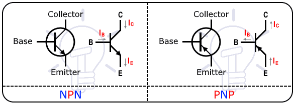 A BJT is made of three alternating layers of P-type and N-type semiconductor materials having two PN junctions. It has 3 terminals i.e. Emitter, Base, and Collector. Each terminal is connected with each layer of the transistor.
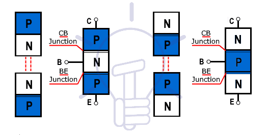 The base is the middle layer sandwiched between Emitter and Collector. The base is the most lightly doped layer of all. The emitter and collector are both heavily doped with the emitter comparatively heavily doped than the collector.BJT is a current controlled device. It means it uses the input current at its base terminal to control the output current or collector current. By connecting the base-collector junction in reverse and base-emitter junction in forward bias allows the flow of current between emitter and collector. This current is directly proportional to the base current.Since its base-emitter junction or input is forward biased, the input impedance is very low. The output impedance is very high due to collector-emitter reverse bias. Therefore, BJT has a very high gain..
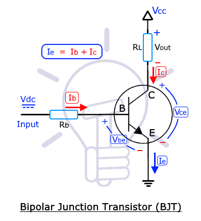 Related Post: Bipolar Junction Transistor (BJT) – Construction, Working, Types & ApplicationsThere are two types of BJTs i.e. NPN and PNP transistor.NPN TransistorNPN Transistor is formed by the combination of two N-type materials and one P-type material. The P-region is sandwiched between N-regions. The three terminals Collector, Base and Emitter each rise from N, P and N regions respectively.The majority charge carriers are electrons while the minority charge carriers are holes. Applying current IB to the base terminal allows current IC from the collector to the emitter. The current is directly proportional to the base current. While the total emitter current IE is the sum of both base Ib and collector current IC.IC = βIBIE = IB + IC
 The symbol of the NPN transistor also represents the direction of the current. The little arrow head pointing outwards of the emitter shows the current direction going outward of the emitter.NPN transistor switches on by applying positive base-emitter voltage VBE and since the majority carriers are electrons, it has a high switching speed.Related Post: What is NPN Transistor? Construction, Working & ApplicationsPNP TransistorThe PNP transistor is formed by the combination of two P-layers and one N-layer. The thin N-layer is sandwiched between two thick P-layers. The middle N-layer is called base while the surrounding two layers are called collector and emitter.
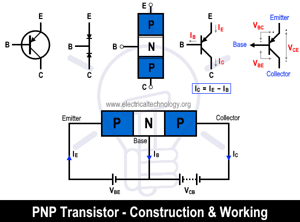 The majority charge carriers are holes while the minority charge carriers are electrons.Reverse biasing collector-emitter junction and forward biasing base-emitter junction puts the transistor into conduction mode where the output current is directly proportional to the base current.PNP transistor switches on when negative voltage VBE is applied to the base region and switches off when a positive voltage is applied.Since the majority carriers are holes, the recovery time of the PNP transistor is comparatively high thus it has low switching speed than the NPN transistor.In the symbol of PNP transistor, the arrowhead pointing inwards represents the direction of the current flowing inside the emitter toward the base and collector. Therefore the total current IC is emitter current minus base current IC = IE – IBRelated Post : What is PNP Transistor? Construction, Working & Applications Field Effect Transistor – FETFET or field-effect transistor is a type of transistor that uses the electric field or voltage to control the current flow. It is unipolar i.e. the current flow only due to majority charge carriers that is either electrons or holes.
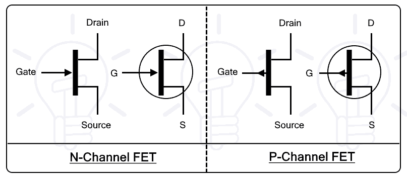 The three terminals of FET are Drain (D), Gate (G) and Source (S). Based on its construction, FET has a channel between its drain and source. The channel refers to the path for the flow of current. The drain and source are made of the same semiconductor material. However, the drain terminal is the one having more positive voltage. Therefore, the drain and source terminals are interchangeable.
 The width of the channel is controlled by the voltage applied at its gate. Applying a forward gate to source voltage VGS increases the channel width and thus the drain current ID. Such mode is called enhancement mode. While applying a reverse VGS decreases the channel length and the current ID. Such operation mode is called depletion mode. Therefore, it is a voltage-controlled device.
 Since the input (gate) is reversed biased, the input impedance of FET is very high in the range of 100M ohm which is why there is no input or gate current. Consequently, it has very low energy consumption and high efficiency. And the output impedance is low. Therefore FET has lesser gain than BJT.Since the FET utilize only one type of charge carrier either electrons or holes, the recovery time is very fast. Therefore, its switching speed is very fast and it can be used for very high-frequency applications.There are two types of FET transistor i.e. JFET (Junction FET) and MOSFET (Metal Oxide Semiconductor FET). Related Post:Difference Between BJT and FET TransistorsDifference Between NPN and PNP TransistorJunction Field Effect Transistor JFETJFET or Junction Field Effect Transistor is a type of FET having one PN junction between the gate and channel. It has three terminals Gate (G), Drain (D) and Source (S). The channel is surrounded by the gate region. The channel and gate are made of the alternating semiconductor layer. The two ends of the channel are named drain and source.
 The channel is built-in during fabrication. Therefore, JFET can conduct current when there is no voltage at its gate. Applying a reverse voltage to the gate creates a depletion region surrounding the channel which pinches and reduces the channel width. The current flow reduces and is eventually stopped when the depletion region completely blocks the channel. Such operation mode is also known as Depletion mode and JFET only works in this mode
 The channel can be made from either P-type or N-type semiconductor material. Therefore, JFET can be divided intoN-Channel JFETP-Channel JFETN-Channel JFETAn N-channel JFET’s channel is made of N-type semiconductor material hence the name. The charge carriers responsible for current flow are electrons. The recovery time of electrons is fast thus N-channel JFET has a fast switching speed.At zero gate voltage, it will conduct current between its source and drain as there is a channel. Applying a negative VGS creates a depletion region that reduces the channel width. Thus, reducing the current flow.P-Channel JFETThe channel in P-channel JFET is made of P-type material and holes are the charge carriers responsible for current flow. Holes are relatively heavier and have a slower speed than electrons. Therefore, P-channel JFET has a slower speed than N-channel JFET.P-channel JFET conducts even when there is no voltage at its gate. Applying a positive gate voltage reduces the channel width and reduces the current flow. Related Posts:Bipolar Junction Transistor (BJT) – Formulas and EquationsTransistor, MOSFET and IGFET SymbolsMOSFETMOSFET or Metal Oxide Semiconductor Field Effect Transistor is a type of FET whose gate terminal is electrically isolated from its channel. Therefore, it is also known as IGFET (Insulated Gate Field Effect Transistor). It has four terminals; drain, gate, source and body. The body terminal is often shorted with the source thus forming three terminals.
 MOSFET has a silicon dioxide insulating layer between its gate and the channel. It increases the input impedance in the range of mega Ohms and reduces the leakage current.
 The MOSFET has the same operation as any other FET. A voltage at its gate is used for varying the channel width and the current through it. It can decrease or increase the width of the channel. Therefore, MOSFET operates in two modes i.e. Depletion mode and Enhancement mode.
 The disadvantage of the insulating layer is that it produces a capacitance between the gate and channel which makes it vulnerable to static charge buildup.Related Post: MOSFET – Working, Types, Operation, Advantages, and ApplicationsDepletion MOSFETDepletion MOSFET or D-MOSFET is a type of MOSFET where the channel is fabricated at the time of manufacturing. It is normally-ON MOSFET that conducts current at no input or gate-source voltage VGS = 0.
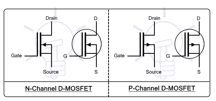 It can operate in both depletion and enhancement mode. Applying forward VGS puts the D-MOSFET into the enhancement mode where the current increases. while applying reverse VGS puts it into depletion mode, where the current decreases and it switches off.
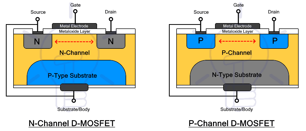 Based on channel, the D-MOSFET can be classified into N-channel and P-channel D-MOSFET.The D-MOSFET can work in both depletion and enhancement mode. While the enhancement MOSFET cannot work in depletion mode.Related Posts:Types of Computer Memory with their ApplicationsTypes of Latches – SR & D LatchesTypes of ICs. Classification of Integrated Circuits and Their LimitationN-Channel D-MOSFETIn N-channel D-MOSFET, the channel is made from N-type material and the current flow is due to electrons. A positive gate-source voltage VGS enhances the channel width thus increasing the current flow. While a negative VGS depletes the channel of charge carriers and reduces the current to completely switch off.
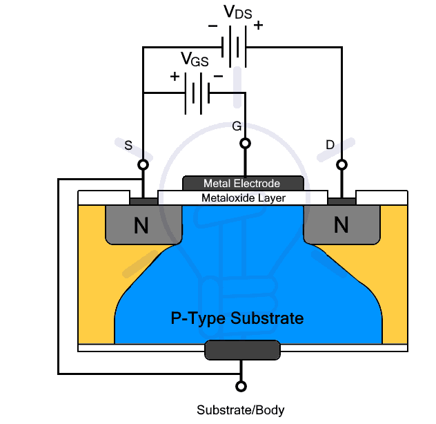 P-Channel D-MOSFETIn P-channel D-MOSFET, the channel is made of P-type material having holes as charge carriers. A positive VGS reduces the channel width and current while a negative VGS enhances the current flow in a P-channel D-MOSFET.Enhancement MOSFETEnhancement MOSFET or E-MOSFET is a “Normally OFF” MOSFET that does not conduct when there is no input. It does not have a channel. The channel is induced by applying forward voltage VGS between its gate and source. The voltage enhances the channel width and the current, hence the name.
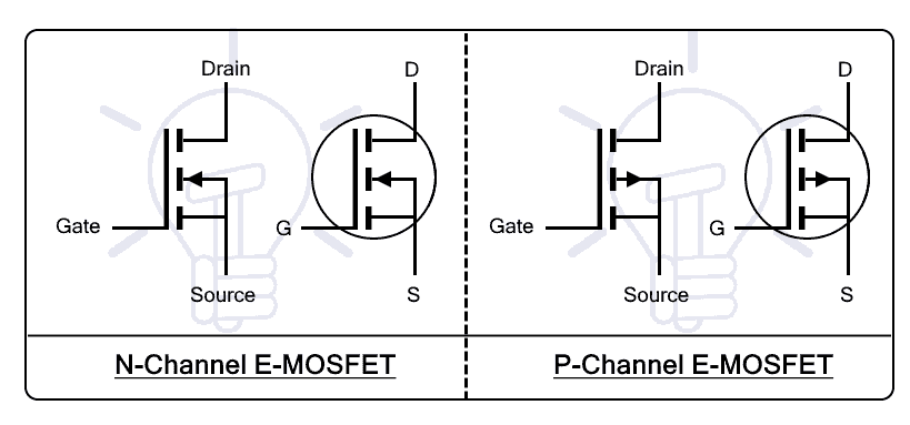 E-MOSFET is also classified into N-channel and P-channel E-MOSFET.N-Channel E-MOSFETThe channel is induced by applying a positive VGS that accumulates a layer of negative charges from the P-substrate beneath its gate that forms the N-channel. Increasing the voltage increases its width and its current conductivity.
 P-Channel E-MOSFETThe channel is induced by applying a negative VGS which enhances the channel width to increase the current flow. The channel is made by accumulating the holes from the N-substrate beneath the gate electrode.
 Related Posts:Difference Between Diode and TransistorDifference Between Transistor & Thyristor (SCR)?Insulated Gate Bipolar Transistor IGBTIGBT or Insulated Gate Bipolar Transistor is a type of transistor that combines the best part of BJT and MOSFET. It has the input characteristics of MOSFET (Insulate Gate) that is high input impedance and fast switching speed and the output characteristics of BJT that is large output current handling capabilities.
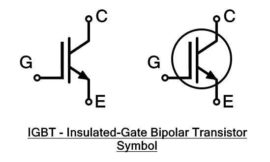 It has three terminals Gate (G), Collector (C) and Emitter (E). The gate represents the MOSFET part while the collector and emitter represent the BJT part. It is a voltage-controlled device like MOSFET having no input current. Thus it has no input losses. However, it is unidirectional, unlike MOSFET which is bidirectional. It allows current only from collector to emitter.
 It is made from the combination of MOSFET and BJT using the Darlington pair configuration as shown above, an N-channel MOSFET with a PNP Transistor. A positive gate-emitter voltage VGE switches ON the MOSFET that starts the base current to the PNP. The PNP switches ON and conducts a huge current.
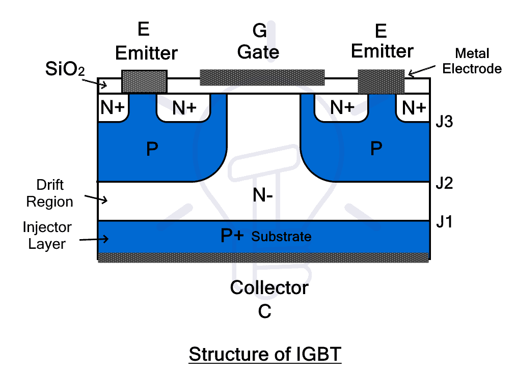 This combination improves the overall voltage and current rating with reduced input losses and a decent switching speed. It is far easier to operate.Related Posts:Thyristor & Silicon Controlled Rectifier (SCR) – Types & OperationWhat is DIAC? Construction & WorkingWhat is TRIC? Construction & OperationPunch through IGBTThe Punch through IGBT has an N+ buffer layer. It has asymmetric voltage blocking capabilities i.e. the forward and reverse breakdown voltages are different. The reverse breakdown voltage is less than the forward breakdown voltage. They cannot handle reverse voltages. They are used in DC circuits since they are unidirectional such as inverters and chopper circuits. It has a faster switching speed
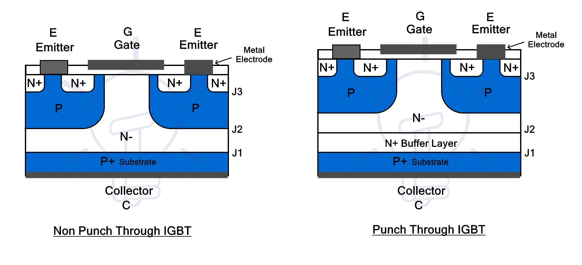 Non Punch through IGBTNon punch through IGBT does not have an N+ buffer layer. They have symmetric breakdown voltage i.e. the forward and reverse breakdown voltages are equal. They are used in AC circuits such as rectifiers.Related Post: How to Check a Transistor by Multimeter (DMM+AVO) – NPN & PNP – 4 WaysSpecial TransistorThere are different kinds of transistors that are designed for special purposes. Here are some of these transistors given below.Darlington Pair TransistorA Darlington transistor or Darlington pair is a combination of two NPN or PNP transistors in such a configuration that their total gain is equal to the product of their individual gain. It provides a very high current gain. The current amplified by the first BJT is amplified by the second BJT. It is used in sensitive circuits and it takes less space than individual transistors.
 The emitter of the first transistor is connected to the base of the second transistor and their collectors are common. It may have a high gain but it also has double base-emitter drops. It is available in a single transistor form having three terminals i.e. base, emitter and collector.Related Posts:Different Types of Sensors with ApplicationsTypes of Filters and Their ApplicationsTypes of Electronic CountersSziklai Pair TransistorSziklai pair just like Darlington pair is a combination of two BJT to improve its current gain. But it combines two different BJTs to from a single transistor. The advantage of this configuration over the Darlington pair is that it has a single base-emitter voltage drop. it has a slightly lower current gain than the Darlington pair.
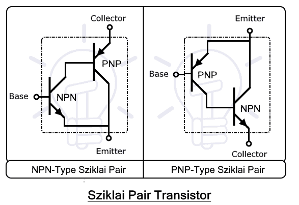 The collector of the first BJT is connected to the base of the second BJT. The emitter of the first and the collector of the second is connected together. The overall Sziklai transistor acts as the first or input transistor. For example, if the first transistor is NPN, the overall transistor would operate as an NPN transistor with high gain. Photo TransistorPhoto Transistor as its name suggests relies on light intensity. It is a simple transistor but instead of the base terminal, there is a light-sensitive region. Therefore, it has only two terminals. The photosensitive region converts the light energy into electrical energy that is used for controlling the output current.
 They can be made of BJT or FET. The BJT photo transistor converts the light energy into the base current while the FET photo transistor converts light into voltage to control the large current.It remains switched off when it is under a shade or there is no light at its photo-sensitive region. It switches on when light falls on its junction that produces the base current or gate voltage proportional to the light intensity. It in turn controls the large collector or drain currentSmall Signal Transistors
 As the name suggests, such transistors are used for amplification and switching of very small signal. They have a very high gain of around 500 and collector’s current rating is in milliamperes. These are very sensitive transistors and must only be used for small signals.Related Posts:Types of Microprocessors & their ApplicationsTypes of Microcontrollers & their ApplicationsSmall Switching TransistorsThese transistors are mainly used for switching small signals. They may be used for amplification; however, their current gain is far less than a small signal transistor in the range of 200. Both transistors are made from BJTs such as NPN and PNP.Power Transistors
Leave a message
Message List
Comments Loading...
