
Products Category
- FM Transmitter
- 0-50w 50w-1000w 2kw-10kw 10kw+
- TV Transmitter
- 0-50w 50-1kw 2kw-10kw
- FM Antenna
- TV Antenna
- Antenna Accessory
- Cable Connector Power Splitter Dummy Load
- RF Transistor
- Power Supply
- Audio Equipments
- DTV Front End Equipment
- Link System
- STL system Microwave Link system
- FM Radio
- Power Meter
- Other Products
- Special for Coronavirus
Products Tags
Fmuser Sites
- es.fmuser.net
- it.fmuser.net
- fr.fmuser.net
- de.fmuser.net
- af.fmuser.net ->Afrikaans
- sq.fmuser.net ->Albanian
- ar.fmuser.net ->Arabic
- hy.fmuser.net ->Armenian
- az.fmuser.net ->Azerbaijani
- eu.fmuser.net ->Basque
- be.fmuser.net ->Belarusian
- bg.fmuser.net ->Bulgarian
- ca.fmuser.net ->Catalan
- zh-CN.fmuser.net ->Chinese (Simplified)
- zh-TW.fmuser.net ->Chinese (Traditional)
- hr.fmuser.net ->Croatian
- cs.fmuser.net ->Czech
- da.fmuser.net ->Danish
- nl.fmuser.net ->Dutch
- et.fmuser.net ->Estonian
- tl.fmuser.net ->Filipino
- fi.fmuser.net ->Finnish
- fr.fmuser.net ->French
- gl.fmuser.net ->Galician
- ka.fmuser.net ->Georgian
- de.fmuser.net ->German
- el.fmuser.net ->Greek
- ht.fmuser.net ->Haitian Creole
- iw.fmuser.net ->Hebrew
- hi.fmuser.net ->Hindi
- hu.fmuser.net ->Hungarian
- is.fmuser.net ->Icelandic
- id.fmuser.net ->Indonesian
- ga.fmuser.net ->Irish
- it.fmuser.net ->Italian
- ja.fmuser.net ->Japanese
- ko.fmuser.net ->Korean
- lv.fmuser.net ->Latvian
- lt.fmuser.net ->Lithuanian
- mk.fmuser.net ->Macedonian
- ms.fmuser.net ->Malay
- mt.fmuser.net ->Maltese
- no.fmuser.net ->Norwegian
- fa.fmuser.net ->Persian
- pl.fmuser.net ->Polish
- pt.fmuser.net ->Portuguese
- ro.fmuser.net ->Romanian
- ru.fmuser.net ->Russian
- sr.fmuser.net ->Serbian
- sk.fmuser.net ->Slovak
- sl.fmuser.net ->Slovenian
- es.fmuser.net ->Spanish
- sw.fmuser.net ->Swahili
- sv.fmuser.net ->Swedish
- th.fmuser.net ->Thai
- tr.fmuser.net ->Turkish
- uk.fmuser.net ->Ukrainian
- ur.fmuser.net ->Urdu
- vi.fmuser.net ->Vietnamese
- cy.fmuser.net ->Welsh
- yi.fmuser.net ->Yiddish
PCB Inspection Techniques & Technologies
- notes and details on maximising manufacturing yields through using electronics inspection technologies including AOI, AXI, etc.
PCB inspection is an essential element in any electronics manufacturing process.
The PCB inspection enables faults to be detected as soon after the manufacture process as possible.
As such the PCB inspection process is an essential element of any PCB manufacturing process.
PCB inspection basics
In the early days of PCB manufacture, or the manufacture of any electronics equipment, all inspection was undertaken manually. This was the best option, but was recognised as having only limited value. The repetitive nature of the process meant that many faults were not spotted and passed on into the next stage of production undetected.
There are various methods by which PCB inspection can be achieved:
•Manual PCB inspection : As the name implies, manual inspection involves individual inspectors looking at boards or other assemblies to inspect them for problems. This approach has been proved to be costly, and yielding poor results. Before automation, it was the only way that inspection could be performed.
•AOI PCB inspection: Automatic or automated optical inspection is the preferred method of PCB inspection. It utilises an optical system that takes an image of a good assembly and compares the two images to detect any faults or other issues.
This form of PCB inspection is widely used and has been perfected so that it operates very reliably.
•AXI PCB inspection: With density on PCBs increasing and new IC mounting technologies being used, not all solder joints may be visible. Particularly when new boards are being manufactured and new set-ups being used, it is very important to check that solder joints on packages such as BGAs (Ball Grid Arrays) are being correctly soldered. Optical inspection cannot achieve this because the solder joints are not visible. The only option is to use an X-Ray system - Automated X-Ray Inspection, AXI, that is able to look under the chips to view the solder joints. Although expensive and only used for a small proportion of the solder joints, etc, they are necessary in many instances.
PCB inspection in a manufacturing process
There are two main uses for a PCB inspection system:
•High light manufacturing defects: The obvious function of a PCB inspection system is to highlight any defects so that they can be corrected before they are passed on to the next stage in the production process. Finding faults as early as possible in the production process is essential because fault finding and fixing costs rise by approximately a factor of ten as each stage in the production process is passed.
•Provide process feedback: An equally important function of a PCB inspection system is to provide feedback into the manufacturing process. Using a PCB inspection system on the output of the soldering process can enable any pattern faults to be seen and the process corrected almost immediately to reduce or eliminate the occurrence of a given problem.
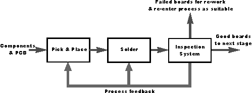
Manufactured PCB production process flow diagram
It can be seen from the diagram, that the PCB inspection process allows boards with failures to be detected as well as feedback to assist the production process to be gained.
