
Products Category
- FM Transmitter
- 0-50w 50w-1000w 2kw-10kw 10kw+
- TV Transmitter
- 0-50w 50-1kw 2kw-10kw
- FM Antenna
- TV Antenna
- Antenna Accessory
- Cable Connector Power Splitter Dummy Load
- RF Transistor
- Power Supply
- Audio Equipments
- DTV Front End Equipment
- Link System
- STL system Microwave Link system
- FM Radio
- Power Meter
- Other Products
- Special for Coronavirus
Products Tags
Fmuser Sites
- es.fmuser.net
- it.fmuser.net
- fr.fmuser.net
- de.fmuser.net
- af.fmuser.net ->Afrikaans
- sq.fmuser.net ->Albanian
- ar.fmuser.net ->Arabic
- hy.fmuser.net ->Armenian
- az.fmuser.net ->Azerbaijani
- eu.fmuser.net ->Basque
- be.fmuser.net ->Belarusian
- bg.fmuser.net ->Bulgarian
- ca.fmuser.net ->Catalan
- zh-CN.fmuser.net ->Chinese (Simplified)
- zh-TW.fmuser.net ->Chinese (Traditional)
- hr.fmuser.net ->Croatian
- cs.fmuser.net ->Czech
- da.fmuser.net ->Danish
- nl.fmuser.net ->Dutch
- et.fmuser.net ->Estonian
- tl.fmuser.net ->Filipino
- fi.fmuser.net ->Finnish
- fr.fmuser.net ->French
- gl.fmuser.net ->Galician
- ka.fmuser.net ->Georgian
- de.fmuser.net ->German
- el.fmuser.net ->Greek
- ht.fmuser.net ->Haitian Creole
- iw.fmuser.net ->Hebrew
- hi.fmuser.net ->Hindi
- hu.fmuser.net ->Hungarian
- is.fmuser.net ->Icelandic
- id.fmuser.net ->Indonesian
- ga.fmuser.net ->Irish
- it.fmuser.net ->Italian
- ja.fmuser.net ->Japanese
- ko.fmuser.net ->Korean
- lv.fmuser.net ->Latvian
- lt.fmuser.net ->Lithuanian
- mk.fmuser.net ->Macedonian
- ms.fmuser.net ->Malay
- mt.fmuser.net ->Maltese
- no.fmuser.net ->Norwegian
- fa.fmuser.net ->Persian
- pl.fmuser.net ->Polish
- pt.fmuser.net ->Portuguese
- ro.fmuser.net ->Romanian
- ru.fmuser.net ->Russian
- sr.fmuser.net ->Serbian
- sk.fmuser.net ->Slovak
- sl.fmuser.net ->Slovenian
- es.fmuser.net ->Spanish
- sw.fmuser.net ->Swahili
- sv.fmuser.net ->Swedish
- th.fmuser.net ->Thai
- tr.fmuser.net ->Turkish
- uk.fmuser.net ->Ukrainian
- ur.fmuser.net ->Urdu
- vi.fmuser.net ->Vietnamese
- cy.fmuser.net ->Welsh
- yi.fmuser.net ->Yiddish
Transistor Configuration Types & Characteristics
Date:2021/10/18 21:55:57 Hits:
Transistors are the basic equipment required for the formation of the devices. Hence the development of these transistors has been a replacement for the vacuum tubes. A basic transistor can be formed by the combination of the p-type semiconductor and the n-type semiconductor. This combination is sandwiched between one p-type and two n-types. The other combination is of two p-types and one n-type. Therefore N-P-N and the P-N-P transistors are formed.These transistors can be classified based on the conduction of which the carrier flow is evident. If the conduction is due to both the majority and the minority charge carriers the transistor is classified to be bipolar. If the conduction is only due to the majority then it is referred to as unipolar. In this way the bipolar junction transistors (BJT) and the field effect transistors (FET) are formed. Transistor Circuit DesignThe transistor is designed in such a way that they consist of three terminals commonly known as emitter, base and the collector. The main reason for designing such configurations is that it requires four terminals in order to provide the input and the output connections of the circuit. Hence this can be made possible by making one terminal in common either it can be base or the emitter or the collector.This designs aims to make the usage of this circuitry in the various applications. The designed configurations based on its requirements are utilized in the electronic modules.Different Configurations of TransistorThree configurations for these transistors are possible known as common base, common emitter and the common collector. Each configuration has its own significance in terms of gain. In the common base configuration there is no current gain but the gain in terms of the voltage is present.In the common collector there is current gain but there will be no voltage gain.The common emitter is the configuration in which both current and the voltage gains are present.Hence the common emitter is the most widely used configurations.1) Common Base Configuration As the name suggests the configuration is of the common terminal base this remains common for both the input and the output circuit connections. The voltage is applied at the junction of the emitter and the base. Here the emitter and the base are referred to as the input side and the collector is known for the output side of the circuit connection.The value of the current flowing from the terminal base to the emitter is must be of the higher value. This indicates the current value at the collector is less than the value of the current flowing through the emitter. The characteristic of the input is based on the voltage applied at the terminals base and the emitter and the current at the emitter terminal. The output characteristic for this configuration is based on the parameters of the voltage applied at the terminals of the base and the collector and the current generated at the collector terminal.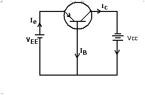 Common Base Configuration The value of the current gain in this case is either equal or considered to be less than the unit value. The signals of the input and the output that are generated will remain in-phase. This kind of configuration has the highest value of the impedance rather than output. The characteristics of the output signals are showcase the similarities as of diode working in forward biased manner.Input CharacteristicsThe input characteristics for this type of configuration is measured by the variation at the voltage value at the terminals of the emitter and the base at different points by keeping the voltage value at the collector and the base as constant. From this the input value of the current that is at emitter is measured. Based on which the graph is plotted.
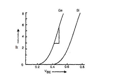 Common Base Input CharacteristicsOutput CharacteristicsThe graph is plotted between the voltage at the output and the current by keeping the input value of the current at the constant gives the output characteristics for this configuration.
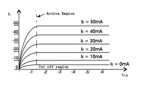 Common Base Output Characteristics 2) Common Collector ConfigurationThis is the configuration in which the collector terminal is made common for both the input and the output connections of the circuit. In this the voltage at the terminal emitter follows the voltage of the base terminal. Hence this circuit is referred to as the emitter following circuit. This kind of the circuitry is helpful in the applications as buffer.
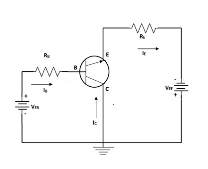 Common Collector ConfigurationThe input value of the impedance is high. Hence these are applicable during the matching of the impedance techniques. The considered input signals are applied in between the terminals of the collector and the base. The output is to be taken or considered in between the terminals of the collector and the emitter.The generated input and the output signals remains in-phase. The input parameters are the voltage between terminals base and the collector and the current at the terminal base. The output parameters are the collector current and the voltage at the terminals emitter and the collector.Input CharacteristicsThe characteristics for this type of configuration are very different in comparison with other configurations. Here the voltage at the collector and the base terminal is determined by the level of the voltage at the emitter and the collector.
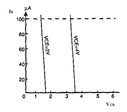 Common Collector Input CharacteristicsBy maintaining voltage at the collector and the emitter at the constant values the graph is plotted between the parameters of the base current and the voltage value at the collector and the base terminals.Output CharacteristicsAs the collector configuration is known to follow the emitter configuration the operation of the output is similar to that of the emitter configuration. In this configuration if there is no voltage is applied at the base terminal there will be no amount of current flow is evident in the circuitry.
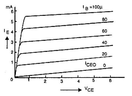 Common Collector Output CharacteristicsThe graph is plotted between the emitter current and the voltage at the terminals of the collector and the emitter by maintaining the value at the base current at constant.3) Common Emitter ConfigurationThis is the most widely used configuration because of the gain in both voltage and the currents increments the gain value of the power. In this the voltage of the input is applied in between the terminals of the emitter and the base. The output is taken across the terminals of emitter and the collector. Hence this circuit of inverting type.
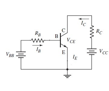 Common Emitter ConfigurationThe parameters of the input for this type of configuration are the voltage at the base and the emitter and the current at the base terminal. The parameters based on which the output signals characterized are the voltage at the terminals of the collector and the emitter as well as the current at the terminal collector.It is the most widely utilized configurations in comparison with the other configurations in the amplifier circuitry. The value of the current at the terminal emitter is the sum of the individual currents at the base and the collector. The impedance at the input as well as the output are of minimum value. This makes the configuration more efficient.The gain between the ratio of current at the collector terminal and the emitter terminal is measured in terms of alpha. The gain for the ratio between the currents of the collector terminal and the base is measured in terms of beta. The generated output signal has the shifting in phase about 180 degrees that represents the input and the output signals are inversely related in terms of phases.Input characteristics The graph is plotted between the current at the base and the voltage value at the terminals of base and the emitter.
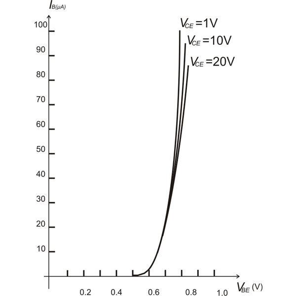 Common Emitter Input CharacteristicsOutput CharacteristicsThe graph is plotted between the values of the collector current and the voltage value of the terminals of collector and the emitter.
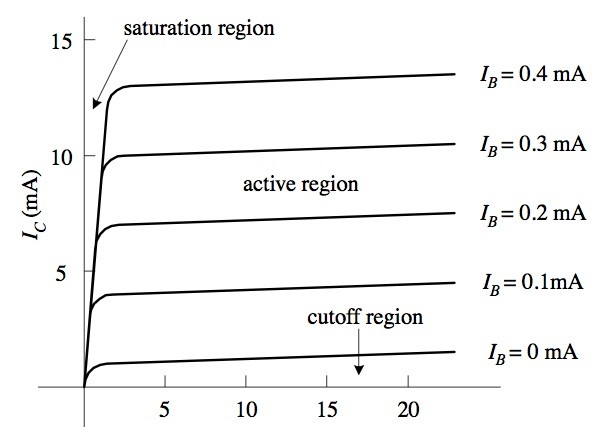 Common Emitter Output CharacteristicsTransistor Configuration Comparison TableBasically a Bipolar Junction Transistor (BJT) consists of the terminals emitter, base and the collector. To these terminals these configurations basing on making one terminal common so that it can act in common for both the input and the output circuits has been designed. Configurations of Transistors Common Base Common Collector Common Emitter 1. The value of Current Gain is Low High Medium 2. The value of Voltage Gain is High Low Medium 3. The value of the Power Gain is Low Medium High 4. The value of the phase relationship between the signals of input and output are Zero Degree Zero Degree 180 Degree 5. Resistance at the Input Low High Medium 6. Resistance at the Output High Low Medium The above there exist three configurations of the transistors based on three terminal present in it. These configurations have certain similarities as well as certain differences in terms of design, input and the output parameters consideration. The values also differ when power, voltage and the current gains are considered. The most frequently used configuration is of common emitter type.It consists of both the voltage and the current gains. Hence it makes the overall power gain high. The common base configuration of the transistor is generally utilized single stage circuits of the amplifier. Hence the configuration of the base that is in common has the highest responses of frequencies. These transistors can be used in amplifiers used in radio frequencies. Can you tell what is the reason that common collector is known as emitter follower?
Leave a message
Message List
Comments Loading...
