Products Category
- FM Transmitter
- 0-50w 50w-1000w 2kw-10kw 10kw+
- TV Transmitter
- 0-50w 50-1kw 2kw-10kw
- FM Antenna
- TV Antenna
- Antenna Accessory
- Cable Connector Power Splitter Dummy Load
- RF Transistor
- Power Supply
- Audio Equipments
- DTV Front End Equipment
- Link System
- STL system Microwave Link system
- FM Radio
- Power Meter
- Other Products
- Special for Coronavirus
Products Tags
Fmuser Sites
- es.fmuser.net
- it.fmuser.net
- fr.fmuser.net
- de.fmuser.net
- af.fmuser.net ->Afrikaans
- sq.fmuser.net ->Albanian
- ar.fmuser.net ->Arabic
- hy.fmuser.net ->Armenian
- az.fmuser.net ->Azerbaijani
- eu.fmuser.net ->Basque
- be.fmuser.net ->Belarusian
- bg.fmuser.net ->Bulgarian
- ca.fmuser.net ->Catalan
- zh-CN.fmuser.net ->Chinese (Simplified)
- zh-TW.fmuser.net ->Chinese (Traditional)
- hr.fmuser.net ->Croatian
- cs.fmuser.net ->Czech
- da.fmuser.net ->Danish
- nl.fmuser.net ->Dutch
- et.fmuser.net ->Estonian
- tl.fmuser.net ->Filipino
- fi.fmuser.net ->Finnish
- fr.fmuser.net ->French
- gl.fmuser.net ->Galician
- ka.fmuser.net ->Georgian
- de.fmuser.net ->German
- el.fmuser.net ->Greek
- ht.fmuser.net ->Haitian Creole
- iw.fmuser.net ->Hebrew
- hi.fmuser.net ->Hindi
- hu.fmuser.net ->Hungarian
- is.fmuser.net ->Icelandic
- id.fmuser.net ->Indonesian
- ga.fmuser.net ->Irish
- it.fmuser.net ->Italian
- ja.fmuser.net ->Japanese
- ko.fmuser.net ->Korean
- lv.fmuser.net ->Latvian
- lt.fmuser.net ->Lithuanian
- mk.fmuser.net ->Macedonian
- ms.fmuser.net ->Malay
- mt.fmuser.net ->Maltese
- no.fmuser.net ->Norwegian
- fa.fmuser.net ->Persian
- pl.fmuser.net ->Polish
- pt.fmuser.net ->Portuguese
- ro.fmuser.net ->Romanian
- ru.fmuser.net ->Russian
- sr.fmuser.net ->Serbian
- sk.fmuser.net ->Slovak
- sl.fmuser.net ->Slovenian
- es.fmuser.net ->Spanish
- sw.fmuser.net ->Swahili
- sv.fmuser.net ->Swedish
- th.fmuser.net ->Thai
- tr.fmuser.net ->Turkish
- uk.fmuser.net ->Ukrainian
- ur.fmuser.net ->Urdu
- vi.fmuser.net ->Vietnamese
- cy.fmuser.net ->Welsh
- yi.fmuser.net ->Yiddish
DIY 300 Watt FM Broadband Amplifier with SD2932 or SD2942
This broadband power amplifier operating over the frequency range 88 - 108 MHz using the new STMicroelectronics RF MOSFET transistor SD2932.
Amplifier design
Input matching networkTypical input gate-to-gate impedance of SD2932 at 100 MHz is Zin = Rs + jXs = 2 - 2.6 j, and can also be expressed as the combination of parallel resistance and reactance using the following formulas:
Equation 1

Equation 2

Therefore, in order to achieve good input matching performances over the frequency range 88-108 MHz the unbalanced 50 Ω is to be transformed into an impedance with a value as close as possible to Rp of 5.38 Ω.
From the circuit schematic given in Figure 3 , we can see that the input matching network is based on a two section balun (1:1 balun in cascade with a 9:1 balun transformer) which transforms the unbalanced 50 Ω to a balanced 5.56 Ω (2 x 2.78 Ω / 9:1 ratio). The first section, a 5" long - 50 Ω coaxial cable and the second section, a two 3.9" long - 25 Ω flexible coaxial cables with ferrite core NEOSIDE, are connected as described: a 10 nH inductor (L1) is connected between the two gates to compensate SD2932 input parallel reactance Xp.
Input matching network tuning
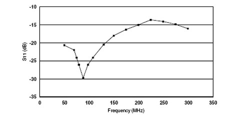
Figure 1. Input Impedance of 1:1 balun in cascade with 4:1 balun

SD2932 input matching network was tuned in order to achieve the best compromise in terms of power gain (Gp) and input return loss (Rtl) over the frequency range 88 - 108 MHz. Best results were achieved by adding a 10 pF chip capacitor (C1) between RFIN and the 1 nF blocking capacitor (C2).
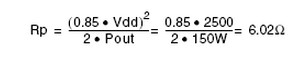
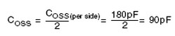
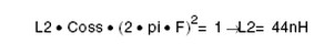
The output impedance of each side is a combination of the output capacitance Coss (195 pF) and the optimum load resistance which can be determined as follows:
Equation 3
The first section, a 5" long - 50 Ω flexible coaxial cable, and the second section, two 5" long - 25 Ω flexible coaxial cables, are connected as described in Figure 3.
Equation 4
Equation 5

Equation 6
Conclusion

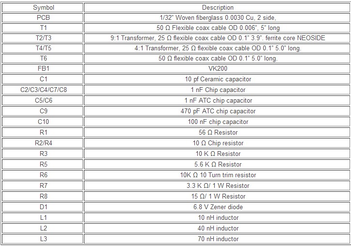
88-108 MHz circuit components list