Products Category
- FM Transmitter
- 0-50w 50w-1000w 2kw-10kw 10kw+
- TV Transmitter
- 0-50w 50-1kw 2kw-10kw
- FM Antenna
- TV Antenna
- Antenna Accessory
- Cable Connector Power Splitter Dummy Load
- RF Transistor
- Power Supply
- Audio Equipments
- DTV Front End Equipment
- Link System
- STL system Microwave Link system
- FM Radio
- Power Meter
- Other Products
- Special for Coronavirus
Products Tags
Fmuser Sites
- es.fmuser.net
- it.fmuser.net
- fr.fmuser.net
- de.fmuser.net
- af.fmuser.net ->Afrikaans
- sq.fmuser.net ->Albanian
- ar.fmuser.net ->Arabic
- hy.fmuser.net ->Armenian
- az.fmuser.net ->Azerbaijani
- eu.fmuser.net ->Basque
- be.fmuser.net ->Belarusian
- bg.fmuser.net ->Bulgarian
- ca.fmuser.net ->Catalan
- zh-CN.fmuser.net ->Chinese (Simplified)
- zh-TW.fmuser.net ->Chinese (Traditional)
- hr.fmuser.net ->Croatian
- cs.fmuser.net ->Czech
- da.fmuser.net ->Danish
- nl.fmuser.net ->Dutch
- et.fmuser.net ->Estonian
- tl.fmuser.net ->Filipino
- fi.fmuser.net ->Finnish
- fr.fmuser.net ->French
- gl.fmuser.net ->Galician
- ka.fmuser.net ->Georgian
- de.fmuser.net ->German
- el.fmuser.net ->Greek
- ht.fmuser.net ->Haitian Creole
- iw.fmuser.net ->Hebrew
- hi.fmuser.net ->Hindi
- hu.fmuser.net ->Hungarian
- is.fmuser.net ->Icelandic
- id.fmuser.net ->Indonesian
- ga.fmuser.net ->Irish
- it.fmuser.net ->Italian
- ja.fmuser.net ->Japanese
- ko.fmuser.net ->Korean
- lv.fmuser.net ->Latvian
- lt.fmuser.net ->Lithuanian
- mk.fmuser.net ->Macedonian
- ms.fmuser.net ->Malay
- mt.fmuser.net ->Maltese
- no.fmuser.net ->Norwegian
- fa.fmuser.net ->Persian
- pl.fmuser.net ->Polish
- pt.fmuser.net ->Portuguese
- ro.fmuser.net ->Romanian
- ru.fmuser.net ->Russian
- sr.fmuser.net ->Serbian
- sk.fmuser.net ->Slovak
- sl.fmuser.net ->Slovenian
- es.fmuser.net ->Spanish
- sw.fmuser.net ->Swahili
- sv.fmuser.net ->Swedish
- th.fmuser.net ->Thai
- tr.fmuser.net ->Turkish
- uk.fmuser.net ->Ukrainian
- ur.fmuser.net ->Urdu
- vi.fmuser.net ->Vietnamese
- cy.fmuser.net ->Welsh
- yi.fmuser.net ->Yiddish
The Principles Of Designing PCB Circuit Board Substrate
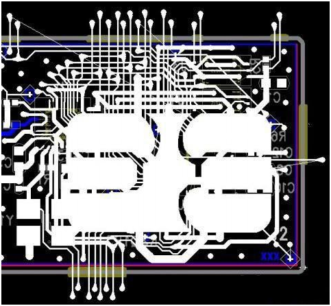
REVIEW: substrate, DIE pads must always bound line direction, and lead wires also needs direction and pads have been, for each DIE, a cross-shaped pad must be placed in its diagonal position As time alignment coordinate binding, which coordinates a network connection required attachments, generally choose to (you must have a network, otherwise the cross will not appear).
DIE bound to note that there is no unused pad removed the need for a network connection. As shown below.
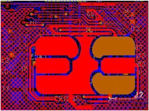
2.Special production process of the substrate, each line must be adopted by the plating line plated brass casting technique as well as the formation of the pads and traces, or all other places need to use copper. Here it must be noted that, even if there is no electrical connection is no network pad, must in eco mode, pull out the pads and frame the exotic copper pads, otherwise the result that no copper pad will appear. And pull out the frame plating lines must have an identity of its position in copper corrosion other layers, where copper is identified by the seventh floor. Generally, the copper beyond the frame by lining 0.15mm, while the distance between the edge of the copper plate and frame shop about 0.2mm distance.
3.Plate frame, to determine the positive and negative, the best all devices are placed on the same side of the face with three XXX logo, as shown below.
4.The substrate used for general pad larger than the pad, there is a special package for the CX0201, X identifies C0201 difference. Are summarized as follows:
0402 Pad: 0.62mmX0.62mm pad fenestration area: 0.5mmX0.5mm, two pads to pitch is 1.0mm.
0201 Pad: 0.42mmX0.42mm pad fenestration area: 0.3mmX0.3mm, two pads to pitch to 0.55mm.
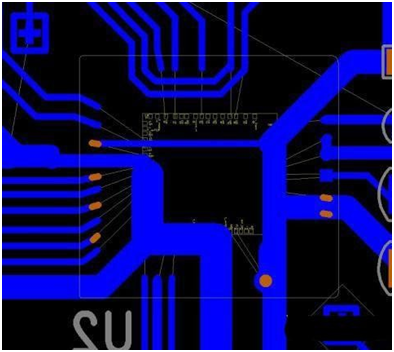
6.Must be maintained between SMT pads and DIE bond pad and SMT components in more than 0.3mm, a binding DIE pad and another should be kept at a distance of more than 0.2mm. Signal traces minimum 2MILS, pitch 2MILS. The main power traces is best to do 6-8MILS, paving the largest possible area. Unable shop where you can shop the power and other signal lines to enhance the strength of the substrate.
7.The wiring should pay attention to via and pad, trace, fingers not from too close, the same properties over Confucius and cheat at least to maintain a 0.12mm or more via different properties as far away from the pad and gold fingers. Via Minimum done outside the bore hole 0.35mm do 0.2mm. Note also that when copper and copper to lay the finger can not be away from the very close, some of the pieces of copper to be deleted, and did not allow a large area to spread to where the presence of copper.
8.When the shop to use copper mesh, the ratio of 1: 4 That COPPERPOUR of 0.4mm to 0.1mm and copper COPPER angle instead of 45 degrees.
Copper is shown.