
Products Category
- FM Transmitter
- 0-50w 50w-1000w 2kw-10kw 10kw+
- TV Transmitter
- 0-50w 50-1kw 2kw-10kw
- FM Antenna
- TV Antenna
- Antenna Accessory
- Cable Connector Power Splitter Dummy Load
- RF Transistor
- Power Supply
- Audio Equipments
- DTV Front End Equipment
- Link System
- STL system Microwave Link system
- FM Radio
- Power Meter
- Other Products
- Special for Coronavirus
Products Tags
Fmuser Sites
- es.fmuser.net
- it.fmuser.net
- fr.fmuser.net
- de.fmuser.net
- af.fmuser.net ->Afrikaans
- sq.fmuser.net ->Albanian
- ar.fmuser.net ->Arabic
- hy.fmuser.net ->Armenian
- az.fmuser.net ->Azerbaijani
- eu.fmuser.net ->Basque
- be.fmuser.net ->Belarusian
- bg.fmuser.net ->Bulgarian
- ca.fmuser.net ->Catalan
- zh-CN.fmuser.net ->Chinese (Simplified)
- zh-TW.fmuser.net ->Chinese (Traditional)
- hr.fmuser.net ->Croatian
- cs.fmuser.net ->Czech
- da.fmuser.net ->Danish
- nl.fmuser.net ->Dutch
- et.fmuser.net ->Estonian
- tl.fmuser.net ->Filipino
- fi.fmuser.net ->Finnish
- fr.fmuser.net ->French
- gl.fmuser.net ->Galician
- ka.fmuser.net ->Georgian
- de.fmuser.net ->German
- el.fmuser.net ->Greek
- ht.fmuser.net ->Haitian Creole
- iw.fmuser.net ->Hebrew
- hi.fmuser.net ->Hindi
- hu.fmuser.net ->Hungarian
- is.fmuser.net ->Icelandic
- id.fmuser.net ->Indonesian
- ga.fmuser.net ->Irish
- it.fmuser.net ->Italian
- ja.fmuser.net ->Japanese
- ko.fmuser.net ->Korean
- lv.fmuser.net ->Latvian
- lt.fmuser.net ->Lithuanian
- mk.fmuser.net ->Macedonian
- ms.fmuser.net ->Malay
- mt.fmuser.net ->Maltese
- no.fmuser.net ->Norwegian
- fa.fmuser.net ->Persian
- pl.fmuser.net ->Polish
- pt.fmuser.net ->Portuguese
- ro.fmuser.net ->Romanian
- ru.fmuser.net ->Russian
- sr.fmuser.net ->Serbian
- sk.fmuser.net ->Slovak
- sl.fmuser.net ->Slovenian
- es.fmuser.net ->Spanish
- sw.fmuser.net ->Swahili
- sv.fmuser.net ->Swedish
- th.fmuser.net ->Thai
- tr.fmuser.net ->Turkish
- uk.fmuser.net ->Ukrainian
- ur.fmuser.net ->Urdu
- vi.fmuser.net ->Vietnamese
- cy.fmuser.net ->Welsh
- yi.fmuser.net ->Yiddish
What Role Does a Power Amplifier(PA) Play in RF?
Date:2019/12/4 15:49:44 Hits:

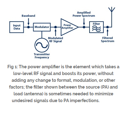
In the RF signal chain, the power amplifier (PA) is the active element located between the transmitter signal chain circuitry and the antenna, Figure 1. It is often a single discrete component, one with requirements and parameters which differ from those of much of the transmit chain as well as the receiver circuitry. This FAQ will look at the role of the PA and how it is characterized.
Q: What does the PA do?
A: The basic function of a PA is very simple in concept. It takes the low-power RF signal, already with the data encoding and modulation and at the desired frequency, and boosts its signal strength to a level necessary for the design. This power level can be anywhere from milliwatts to tens, hundreds, or thousands of watts. The PA does not change the signal shape, format, or mode, but “merely” amplifies it.
Q: Is the PA always an independent, discrete component?
A: No. For lower-power RF output on the order of 100 mW or less, the PA may be a part of the RF transmit IC or even the larger transceiver IC. While implementing the PA this way may save BOM cost, it does require the designer to be very careful about physical placement of the RF IC and the antenna, as RF signal routing is a challenge. Also, the design and execution of the on-chip PA may force difficult compromises on its performance or the performance of the associated RF circuitry.
At the other extreme of higher-power levels on the order of 500-1000 W, a single discrete PA may not be capable of handling the power level. In these cases, multiple PA devices may be used in parallel. While doing so can solve the power problem, a parallel design brings the new issue of power balance, current sharing, thermal matching, dealing with and preventing individual failures or overheating, and more.
Q: What’s a MMIC?
A: An RF IC with or without the PA is soenti9es referred to as a MMIC– millimeter IC – although strictly speaking, millimeter waves span 30 GHz to 300 GHz, while the range from 1 GHz to 30 GHz is considered microwaves. But common usage often uses the term MMIC for the higher microwave frequencies.
Q: What semiconductor processes are used for RF PAs?
A: In addition to standard MOSFETs, until about a decade ago, the dominant process was gallium arsenide (GaAs), and it is still used today, mostly in the <5 W range of smartphones and cable TV. At higher power levels, gallium nitride (GaN) has made significant progress in the past decade, due to both market needs and significant process investment by vendors. GaN is now the most-favored PA process for new designs.
Q: How does operating frequency enter into the situation?
A: Whenever there is an RF design, the key issues are power and frequency, and the impact of one factor on the other. FETs work beat up to several hundred MHz but can reach into the GHz range, while GaAs is useful to several tens of GHz, although best under 10 GHz. At frequencies into the several tens of GHz, where much of the emerging RF activity is focused (think 5G), GaN is the most attractive process. (Of course, every one of these general statements has exceptions, plus the entire area is fast moving, so these general statements are in flux.)
Note that process technology is only part of the story. The other part is how the process is used, in terms of fabrication topology, Among the options are bipolar junction transistors (BJTs), enhancement-mode MOSFETs, heterojunction bipolar transistors (HBTs), metal-semiconductor FETs (MESFETs), high electron mobility transistors (HEMTs), and laterally diffused metal oxide semiconductors (LDMOS). The subtleties of each are generally not directly relevant to the PA user, but they do affect what the PA can do and its limitations.
Q: Assuming the PA has the right specifications, what are the primary design-in issues affecting its use?
A: There are three: layout, signal integrity, and parasitics; thermal management (PA efficiency can be anywhere from 30% to 70%, typically), heat sink, air flow, and conductive/convention cooling; and developing a network for impedance matching to the antenna, Figure 2.
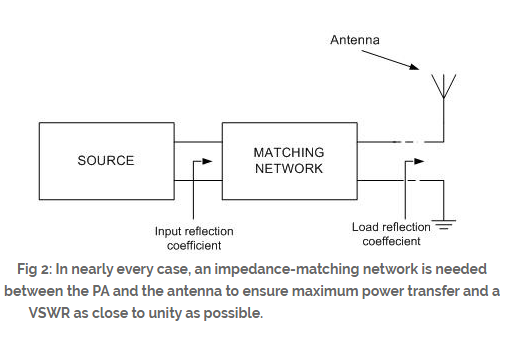
Q: Layout and thermal management seem straightforward enough to anticipate and model, but what about matching?
A: Matching is tricky because an acceptable match – one that results in a VSWR <2 in most cases – requires careful modeling, use of the Smith chart (Figure 3) or similar tool, and often a VNA (vector network analyzer). But the real challenge is that the parameters of the load – here, the antenna – may not be constant.
If the end product is a smart phone, for example, the placement of the user’s hands and body, as well as other nearby objects, affects the load impedance and thus the goodness of the impedance match. As circumstances change during use, the antenna “detunes” and VSWR will increase, leading to radiated-energy inefficiency, possible overheating, and thermal shutdown. Here are techniques available to counteract these shifts such as dynamic impedance matching, but these add cost and complexity.
If you are interested in Power Amplifier and FM/TV Transmitter Equipment, please feel free to contact us:[email protected] .
Leave a message
Message List
Comments Loading...
