
Products Category
- FM Transmitter
- 0-50w 50w-1000w 2kw-10kw 10kw+
- TV Transmitter
- 0-50w 50-1kw 2kw-10kw
- FM Antenna
- TV Antenna
- Antenna Accessory
- Cable Connector Power Splitter Dummy Load
- RF Transistor
- Power Supply
- Audio Equipments
- DTV Front End Equipment
- Link System
- STL system Microwave Link system
- FM Radio
- Power Meter
- Other Products
- Special for Coronavirus
Products Tags
Fmuser Sites
- es.fmuser.net
- it.fmuser.net
- fr.fmuser.net
- de.fmuser.net
- af.fmuser.net ->Afrikaans
- sq.fmuser.net ->Albanian
- ar.fmuser.net ->Arabic
- hy.fmuser.net ->Armenian
- az.fmuser.net ->Azerbaijani
- eu.fmuser.net ->Basque
- be.fmuser.net ->Belarusian
- bg.fmuser.net ->Bulgarian
- ca.fmuser.net ->Catalan
- zh-CN.fmuser.net ->Chinese (Simplified)
- zh-TW.fmuser.net ->Chinese (Traditional)
- hr.fmuser.net ->Croatian
- cs.fmuser.net ->Czech
- da.fmuser.net ->Danish
- nl.fmuser.net ->Dutch
- et.fmuser.net ->Estonian
- tl.fmuser.net ->Filipino
- fi.fmuser.net ->Finnish
- fr.fmuser.net ->French
- gl.fmuser.net ->Galician
- ka.fmuser.net ->Georgian
- de.fmuser.net ->German
- el.fmuser.net ->Greek
- ht.fmuser.net ->Haitian Creole
- iw.fmuser.net ->Hebrew
- hi.fmuser.net ->Hindi
- hu.fmuser.net ->Hungarian
- is.fmuser.net ->Icelandic
- id.fmuser.net ->Indonesian
- ga.fmuser.net ->Irish
- it.fmuser.net ->Italian
- ja.fmuser.net ->Japanese
- ko.fmuser.net ->Korean
- lv.fmuser.net ->Latvian
- lt.fmuser.net ->Lithuanian
- mk.fmuser.net ->Macedonian
- ms.fmuser.net ->Malay
- mt.fmuser.net ->Maltese
- no.fmuser.net ->Norwegian
- fa.fmuser.net ->Persian
- pl.fmuser.net ->Polish
- pt.fmuser.net ->Portuguese
- ro.fmuser.net ->Romanian
- ru.fmuser.net ->Russian
- sr.fmuser.net ->Serbian
- sk.fmuser.net ->Slovak
- sl.fmuser.net ->Slovenian
- es.fmuser.net ->Spanish
- sw.fmuser.net ->Swahili
- sv.fmuser.net ->Swedish
- th.fmuser.net ->Thai
- tr.fmuser.net ->Turkish
- uk.fmuser.net ->Ukrainian
- ur.fmuser.net ->Urdu
- vi.fmuser.net ->Vietnamese
- cy.fmuser.net ->Welsh
- yi.fmuser.net ->Yiddish
PMOS and NMOS Transistors
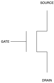
Microprocessors are built of transistors. In particular, they are constructed out of MOS transistors. MOS is an acronym for Metal-Oxide Semiconductor. There are two types of MOS transistors: pMOS (positive-MOS) and nMOS (negative-MOS). Every pMOS and nMOS comes equipped with three main components: the gate, the source, and the drain.
To properly understand how a pMOS and an nMOS operate, it is important to first define some terms:
closed-circuit: This means that the electricity is flowing from the gate to the source.
open-circuit: This means the electricity is not flowing from the gate to the source; but rather, electricity is flowing from the gate to the drain.
When an nMOS transistor receives a non-negligible voltage, the connection from the source to the drain acts as a wire. Electricity will flow from the source to the drain uninhibited — this is referred to as a closed-circuit. On the other hand, when an nMOS transistor receives a voltage at around 0 volts, the connection from the source to the drain will be broken and this is referred to as an open-circuit.
The p-type transistor works exactly counter to the n-type transistor. Whereas the nMOS will form a closed-circuit with the source when the voltage is non-negligible, the pMOS will form an open-circuit with the source when the voltage is non-negligible.

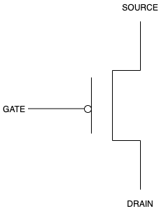
As you can see in the image of the pMOS transistor shown above, the only difference between a pMOS transistor and an nMOS transistor is the little circle between the gate and the first bar. This circle inverts the value from the voltage; so, if the gate sends a voltage representative of a value of 1, then the inverter will change the 1 to a 0 and cause the circuit to function accordingly.
Since pMOS and nMOS function in an opposite manner — in a complementary manner — when we combine the both of them into one giant MOS circuit, it is called a cMOS circuit, which stands for complementary metal-oxide semiconductor.
Utilizing the MOS Circuits
We can combine pMOS and nMOS circuits in order to build more complex structures called GATES, more specifically: logic gates. We have already introduced the concept of these logical functions and their associated truth tables in the previous blog, which you can find by clicking here.
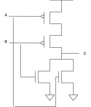
We can attach a pMOS transistor that connects to the source and an nMOS transistor that connects to the ground. This will be our first example of a cMOS transistor.

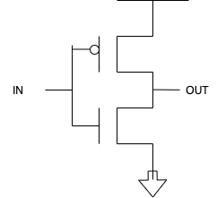
This cMOS transistor acts in a manner similar to the NOT logical function.
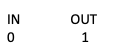
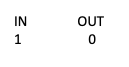
Let’s take a look at the NOT truth table:

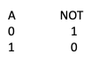
In the NOT truth table, every input value: A is inverted. What happens with the circuit above?
Well, let’s imagine the input is a 0.
The 0 comes in and goes both up and down the wire to both the pMOS (top) and the nMOS (bottom). When the value 0 reaches the pMOS, it gets inverted to a 1; so, the connection to the source is closed. This will produce a logical value of 1 so long as the connection to the ground (drain) is not also closed. Well, since the transistors are complementary, we know that the nMOS transistor won’t invert the value; so, it takes the value 0 as is and will — therefore — create an open circuit to the ground (drain). Thus, a logical value of 1 is produced for the gate.

What happens if a 1 is the IN value? Well, following the same steps as above, the value 1 gets sent to both the pMOS and the nMOS. When the value is received by the pMOS, the value gets inverted to a 0; thus, the connection to the SOURCE is open. When the value is received by the nMOS, the value does not get inverted; thus, the value remains a 1. When a value of 1 is received by the nMOS, the connection is closed; so, the connection to the ground is closed. This will produce a logical value of 0.

Putting the two sets of input/output together yields:

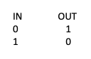
It is quite easy to see that this truth table is the exact same as that which the logical function NOT produces. Thus, this is known as a NOT gate.
Can we use these two simple transistors to make more complicated structures? Absolutely! Next, we will build a NOR gate and an OR gate.

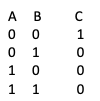
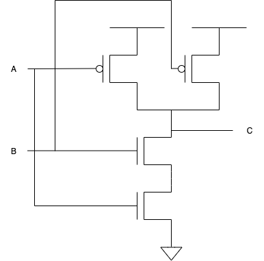
This circuit uses two pMOS transistors at the top and two nMOS transistors at the bottom. Again, let’s look at the input to the gate to see how it behaves.
When A is 0 and B is 0, this gate will invert both the values to a 1 when they reach the pMOS transistors; however, the nMOS transistors will both maintain the value of 0. This will lead the gate to produce a value of 1.
When A is 0 and B is 1, this gate will invert both the values when they reach the pMOS transistors; so, A will change to 1 and B will change to 0. This will not lead to the source; since both of the transistors require a closed-circuit in order to connect the input to the source. The nMOS transistors do not invert the values; so, the nMOS associated with A will produce a 0, and the nMOS associated with B will produce a 1; thus, the nMOS associated with B will produce a closed circuit to the ground. This will lead the gate to produce a value of 0.
When A is 1 and B is 0, this gate will invert both the values when they reach the pMOS transistors; so, A will change to 0and B will change to 1. This will not lead to the source; since both of the transistors require a closed-circuit in order to connect the input to the source. The nMOS transistors do not invert the values; so, the nMOS associated with A will produce a 1, and the nMOS associated with B will produce a 0; thus, the nMOS associated with Awill produce a closed circuit to the ground. This will lead the gate to produce a value of 0.
When A is 1 and B is 1, this gate will invert both the values when they reach the pMOS transistors; so, A will change to 0 and B will change to 0. This will not lead to source; since both of the transistors require a closed-circuit in order to connect the input to the source. The nMOS transistors do not invert the values; so, the nMOS associated with A will produce a 1, and the nMOS associated with B will produce a 1; thus, the nMOS associated with A and the nMOS associated with B will produce a closed circuit to the ground. This will lead the gate to produce a value of 0.
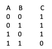
Thus, the gate’s truth table is as follows:

Meanwhile, the NOR logical function’s truth table is as follows:

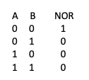
Thus, we have confirmed that this gate is a NOR gate because it shares its truth table with the NOR logical function.
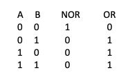
Now, we will put both of the gates, that we have created thus far, together in order to produce an OR gate. Remember, NOR stands for NOT OR; so, if we invert an already inverted gate, we will get back the original. Let’s put this to the test in order to see it in action.

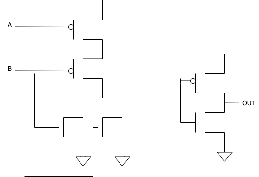
What we have done here is we’ve taken the NOR gate from before and applied a NOT gate to the output. As we have shown above, the NOT gate will take a value of 1 and output a 0, and the NOT gate will take a value of 0 and output a 1.
This will take the values of the NOR gate and convert all of the 0s to 1s and 1s to 0s. Thus, the truth table will be as follows:

If you would like more practice testing these gates, feel free to try out the above values for yourself and see that the gate produces equivalent results!

I claim this is a NAND gate, but let’s test this gate’s truth table to determine if it really is a NAND gate.
When A is 0 and B is 0, A’s pMOS will produce a 1, and A’s nMOS will produce a 0; thus, this gate will produce a logical 1 since it is connected to the source with a closed circuit and disconnected from the ground with an open circuit.
When A is 0 and B is 1, A’s pMOS will produce a 1, and A’s nMOS will produce a 0; thus, this gate will produce a logical 1 since it is connected to the source with a closed circuit and disconnected from the ground with an open circuit.
When A is 1 and B is 0, B’s pMOS will produce a 1, and B’s nMOS will produce a 0; thus, this gate will produce a logical 1 since it is connected to the source with a closed circuit and disconnected from the ground with an open circuit.
When A is 1 and B is 1, A’s pMOS will produce a 0, and A’s nMOS will produce a 1; so, we must check B’s pMOS and nMOS, as well. B’s pMOS will produce a 0, and B’s nMOS will produce a 1; thus, this gate will produce a logical 0 since it is disconnected from the source with an open circuit and connected to the ground with a closed circuit.
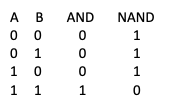
The truth table is as follows:

Meanwhile, the NAND logical function’s truth table is as follows:

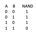
Thus, we have verified that this is, indeed, a NAND gate.
Now, how do we build an AND gate? Well, we will build an AND gate the exact same way we built an OR gate from a NOR gate! We will attach an inverter!

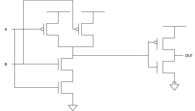
Since all we have done is applied a NOT function to a NAND gate’s output, the truth table will look like this:

Again, please verify to make sure that what I am telling you is the truth.
Today, we have covered what are pMOS and nMOS transistors as well as how to use them to build more complex structures! I hope you found this blog informative. If you would like to read my previous blogs, you will find the list below.
